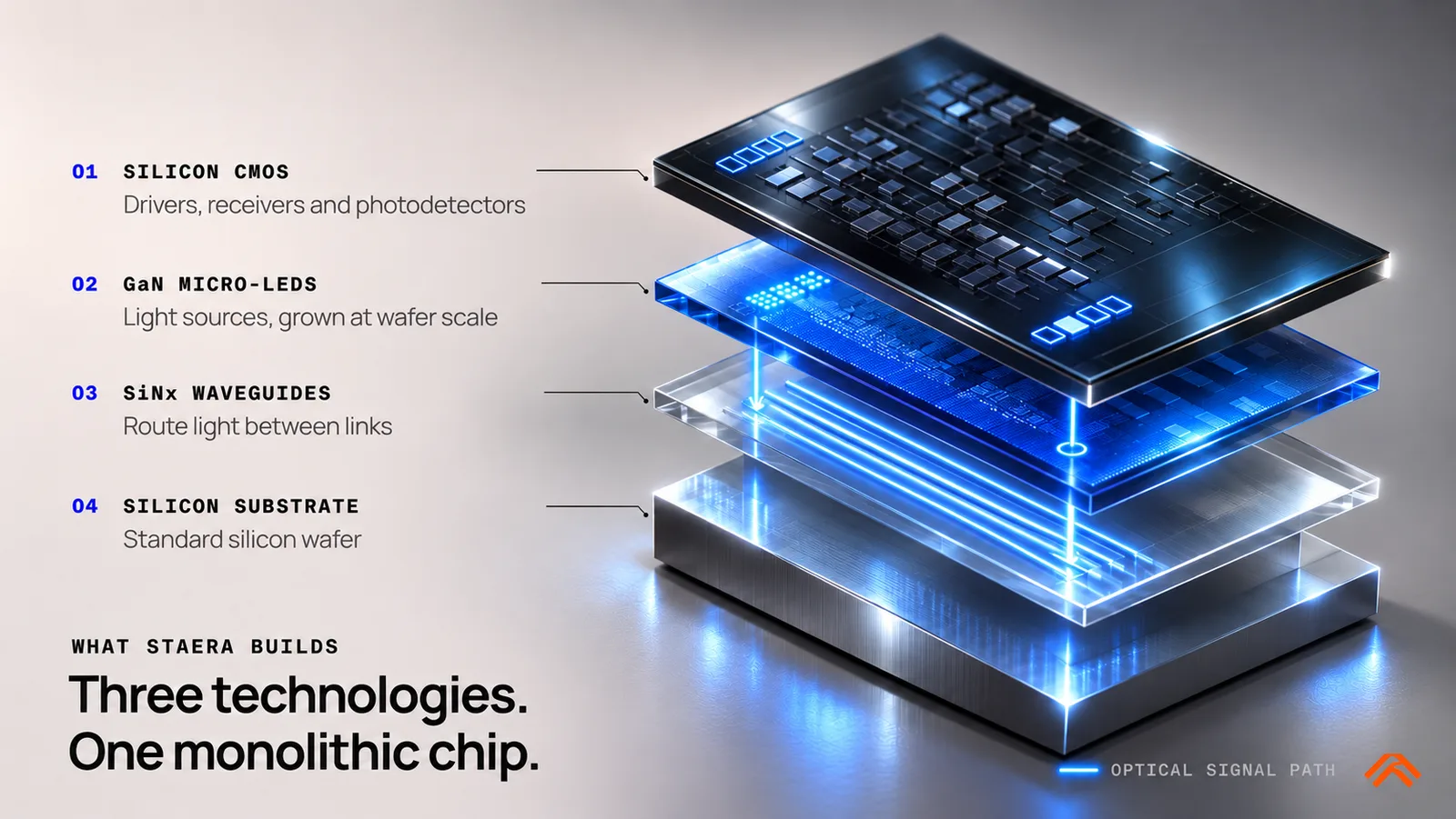
Staera Semiconductor, a startup that builds LED-based optical data links inside silicon chips, raised US$4.6m in pre-seed funding as it came out of stealth on 10 November 2026.
Openspace Capital led the round, with SGInnovate, Black Kite Capital, 28 Holdings, In Group and Decimus Technologies also investing. The company, previously known as New Silicon Corporation, did not disclose a valuation.
Reports differ on where Staera is based. Its announcement carried a San Francisco dateline and SiliconANGLE described it as a San Francisco company, while TNGlobal and DealStreetAsia called it Singapore-based. TNGlobal reported that it began as a spin-off from the Low Energy Electronic Systems research group at the Singapore-MIT Alliance for Research and Technology.
“AI's bottleneck is no longer how fast chips compute, but how fast and far they can move data.”Andrew Kim, Chief Executive Officer, Staera Semiconductor
The problem with copper
High-end AI accelerators are assembled from several chiplets, small dies that are wired together through a base layer called an interposer or a smaller, cheaper version known as a bridge. Those connections use copper. Staera says copper's electrical performance falls by a factor of a thousand between one millimetre and one metre, the distances that separate chips, boards and racks.
Optical links already exist, but they are usually separate lasers or LEDs made elsewhere and mounted beside the chip. Staera argues that this adds power and complexity. The company also cites an International Energy Agency forecast that data-centre electricity use will more than double, from about 415 terawatt-hours in 2024 to around 945 terawatt-hours by 2030.
How Lightwire works
Staera's first product, Lightwire, puts the whole optical link inside the chip. It combines three technologies on one silicon wafer: standard CMOS circuits, gallium nitride LEDs that produce the light, and silicon nitride waveguides that carry it. Because it sits inside the interposer or bridge that already joins processors and memory, the company says it fits existing packaging and can be made in existing fabs.
The company's design targets include 4 to 8 gigabits per second per link, more than 600 links per millimetre of chip edge and energy use below 0.2 picojoules per bit, against 5 picojoules for co-packaged optics. Staera says moving 24 terabytes a second would take under 50 watts with Lightwire, compared with close to a kilowatt using co-packaged optics. It also says it has made GaN LEDs inside silicon chips at commercial foundries since 2016, with yields of 98% to 99%.
None of this is on sale yet. Staera is aiming for a commercial release in 2030.
The team
Chief executive Andrew Kim worked on LED products at Lumileds and later co-founded Glint Lighting, which he led through an exit in 2024, according to the company's website. Chief scientist Kenneth Lee spent 12 years in Singapore's defence research sector before leading the SMART research group where Staera's technology was developed. The chairman, MIT professor Eugene Fitzgerald, developed strained silicon and commercialised it through his earlier startup, AmberWave.
In May 2026 Staera won the startup competition at the IEEE Electronic Components and Technology Conference and was runner-up in the Lam Capital Venture Competition run by Lam Research.
What the money is for
Staera said the round marks its move from research to a commercial product. It plans to develop the technology further, expand its team into the US and work more closely with customers and supply-chain partners. SiliconANGLE reported that the company also intends to build out a manufacturing supply chain.
Hian Goh, co-founder of Openspace Capital, said the firm invested because of Staera's technology, the depth of its team and its potential to create a new category in chip connectivity. Staera did not disclose its headcount or any earlier funding.
Company website: staera.ai